I prefer to pour a ground-plane on both sides (top and bottom). Eagle will figure out where it makes sense to have one, and where the circuit becomes too busy. You can end up with lots of vias doing this though, so YMMV. For me, it means I mill less copper
")
If you do pour copper on 2 sides, you can put vias close by the heating elements (excuse me: chips) and they can dissipate heat on two copper planes, not one.
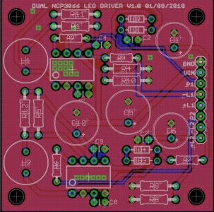
Done. I put vias under the ICs and in a few other strategic places so the top GND layer wouldn't be so broken up. Is that a good idea, or should I just let it have big voids where traces are breaking up?
If you're getting this board made professionally, it doesn't really matter because the holes will be plated-through, but putting tRestrict boxes around the hidden solder points (eg: under the capacitors) will make it easier for the home-brewer because they can then be soldered from the non-component side.
It'll be made professionally. In the "production" run at least. I want to get two or three boards as prototypes but I'm stuck in what's probably a classic debate - do I pay a bunch per board to get two prototypes from a board house, or try to make them myself? Or, do I have the guts to just order 40 of them and cross my fingers?

I prefer to not run traces along the edge of the board (see JP2).
Moved the connector back. The header I used is just a .1" pin header. I don't think I want that in the final product, so I may switch it out alltogether. What would you all use for a connector on the final product? Screw terminals?
Since you're not space-constrained, I might bump-up the separation between tracks/vias in the aurorouter - D1 looks like it doesn't need to be so close, for example. This is nit-picking though...
I saw D1 and moved that trace right after posting. I actually routed this by hand. The autorouter did a lot of things I didn't like. But then again, I don't know if what I like is good or not.
I tend to put a revision number as text on the top, so I know whether the circuit is the latest version, 3 months later
Good idea. Done. I'm naming each version of the file but I suppose it makes sense to have an obvious link to the real world version, too.
I might make the tracks a little wider, just to be sure.
I've bumped up a bunch of the traces up that will be carrying power to both ICs. They should be overkill now. 40 mils. Then 32 mils on some of the power-carrying traces that only serve one IC. 24 mils for everything else except the PWM signal traces, which I think I left at 12 mils.
- I would suggest you skip tValues and just place tNames inside the blueprint of the part where possible and close to it where not. It makes it very easy to populate with just a BOM.
That's what I'll do for a final product. The names and values on there now are by virtue of the parts I used from libraries included with Eagle or other sources. This is a silly question, but I can't figure out how to edit or move that "automatically generated" text (i.e. moving it with respect to the part) without going back and editing the part in the library. I suppose I could just hide those layers and put plain text on myself?
The caps you are using are polarized, so please indicate which pin is positive :
Will do when I figure out the name/value labels.
1) I'll add agreement with board edge traces. You can have them but keep them back from the edges 50mil. Move that connector inboard a little.
Done. They're all now at least 50 mils from the edge.
Now you're fooling with me. :lol: (right?)
It also causes etching problems as the inside corners hold etchant and over-etch.
That makes sense. I'll try to eliminate the right angles.
3) Label some test points even if they just point to a resistor lead or something. V+, GND, etc.
I've labeled the header now, at least.
4) Turn R5 and its pal 90 degrees.
Done.
5) In every case where you have a big cap and you run the trace by sending a diagonal off to a cap lead - don't. Run the trace thru the cap lead directly. If you have some procedural issue with this then make the stubs as short as you can.
Done. I've heard lots of "advice" on cap placement and how the way you run traces to them can screw things up, but it's never been clear. I appreciate the clarity.
C1 is a disaster in the making BTW.
Because of the above, or something else?
6) I don't know about that NCP chip but usually you want bypass caps associated with most ICs. I see none. (0.1uF)
Maybe because the names/values aren't clear, but the caps connected to the VIN pin on each IC, pin 6, (C9 and C4) are .1uF ceramics for bypassing.
Oh, you could cut that board down by at least a 1/3 possibly 1/2 if you wanted to.
I figured, but made it 5cm x 5cm because that gave a bit more wiggle room. Plus, the board house I'm planning on using has a 5cm x 5cm minimum, so if I made it any smaller it wouldn't be any cheaper, anyways. Is there a compelling reason to make a circuit more compact, other than that it'll take up less space?
If I do produce a working PCB from this design, are others considering using it? I'm assuming so, and hence trying to design for a general audience and not just me. Hence the larger board size allowing for nicer spacing between components, plus something related to my next question. I've doubled up the two tricky resistors on each driver (Rsense and the peak current resistor) in case me or others make this and need to parallel resistors to get the right final value. I had to do that in some of my prototypes so I figured it was worth including. Any compelling reason to not do that in a final product?
Also, another question. Since I'm doubling up, what do I do with the caps on the power input side? As a single driver, it's fine with a big electrolytic cap (220uF) and a little bypass ceramic cap (.1uF). I'm assuming I should keep the bypass for each IC, but do I need two of the big caps? Or, just one giant cap? I've designed it with two 220uF caps, but there's a whole range with the same footprint and pin spacing so I suppose people could change values if they needed to. Or leave one out and just use a single large cap. Thoughts anyone?