Looks Good!
I like the symmetry.
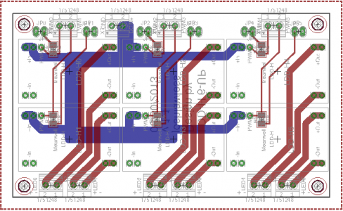
1) I would make the output trace widths minimum 76 mil or better yet 100 mil. you have plenty of room.
2) The DCIN+ traces from the "square buss" to the LDD's could be increased to 100mil. They should be minimum 76 mil.
3) You can eliminate the X8 screw terminal assuming the terminal you spec'd will handle max current. If not I would split LDD 0-2 and LDD 3-5 and use two separate power supplies. Paralleling X7 and X8 does not necessarily mean the load will be split equally.
4) I would eliminate the bottom ground plane.
There is really no need for top and bottom ground planes in this circuit.
In high frequency circuits (not this one) this can cause problems.
5) Minor, but worth consideration. You have the pull up resistors placed under the LDD's. With this configuration the LDD's will not sit flush on the board.
You may want to think about moving the resistors or LDD's. Possibly move the resistors to the bottom side of the board.
Impressive work.
-BB
 id=1751248&library=usen&pcck=P-11-01-01&tab=1


