Here is the first run at it.
Few comments:
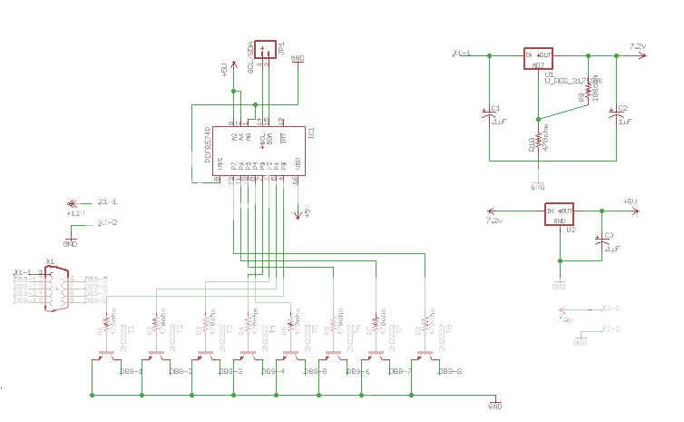
1) As noted above, I think it would be a good approach to standardize on the MCP23008 for GPIO expansion, so we can keep the code universal. Otherwise there's nothing wrong with that chip you picked.
2) Also as noted earlier, I'd rather see the address pins set up with jumpers or solder bridges to GND and 5v so you can choose any address you want.
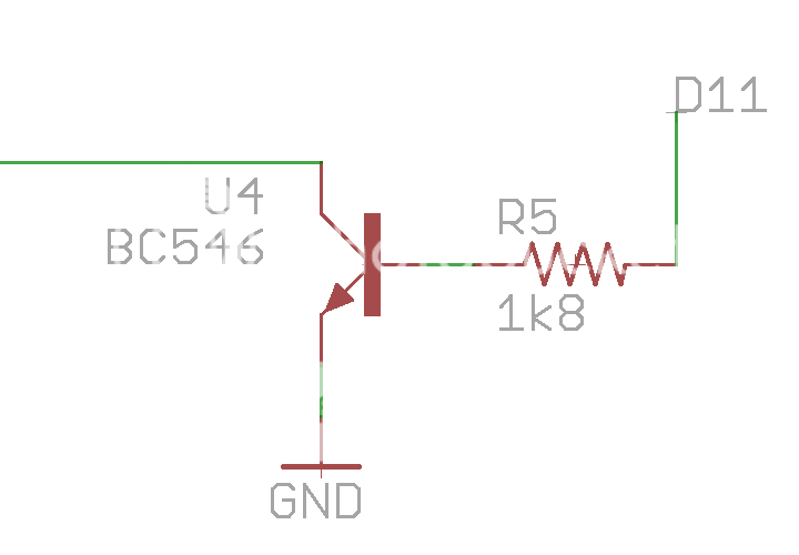
3) Not enough caps on that board! Just about ANY active IC should always have a .1uF ceramic cap right next to it's power pin(s). In other words, you need one on the port expander. It's also generally considered good practice to put one on each side of a linear reg (the 7805 and 317). Also I think you want to check the values/types of the caps you have drawn in the schematic. You're showing a .1uF electrolytic for C1 and C3, and a 1uF electrolytic for C2. Those aren't really typical values or types for this sort of application. Check out the caps around the voltage regs on the mainboard to get an idea.
4) You may be able to find a linear reg with a fixed output voltage to use instead of the LM317. That would reduce parts count by two (the resistors to set the voltage for the LM317). Not a big deal in terms of cost but it frees up board space.
5) For C1, C2, and C3, make sure you can easily get electrolytic caps in the capacitances and voltages you need in that package size - you need to check pin spacing and diameter of the cap. Otherwise it would suck to get the boards made and then have a hard time finding caps to fit. If you look at the caps and package sizes used on the main Hydra board you can get an idea for what's available, as I tried to only use stuff that was really easy to get.
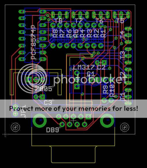
6) I think you could get a little simpler with your layout if you wanted to (I don't think you NEED to, but I think it's actually fun to try). I'd try to physically arrange things according to the "flow" of the circuit. Put power management "first" with the GPIO chip next to it. Then put the resistors next to the IC, and the transistors on the other side of the resistors. Then put the output header (the DB9 connector) on the other side of the transistors. This could really cut down on the complexity of the traces. Also, it's probably not strictly required, but I don't see a reason to not have a ground plane on the top and bottom of the board.
7) If you're going to release the design with the hopes of sharing with others (I hope you do!) then I would suggest adding some descriptive text - it can be a few words. Also, might want to put your name somewhere on the board, as well as a version number and release date. This way, if the design ever changes, it'll be obvious which physical PCBs match which versions of the design files.
8) I would definitely like to see any expansion boards use the same pinout as on the mainboard for communications (I2C in this case) - so as Dustin suggested, it would be nice to see a 4-pin header including 5v and GND on your board instead of just the 2 pin SDA and SCL header you have on there now.
Which brings up another point I've been thinking about. Power management. I see you guys are using a reg on your breakout boards to generate a "raw" 7.2v to feed the power input on the mainboard? And, you're generating 5v on your breakouts? I get the thought process but it seems to me like there is some room for confusion if we don't have a standard approach to what/where/how power is managed. For instance, I know the 5v reg on the mainboard is going to be pretty taxed as it is, but do we really need or want to generate 5v to power a GPIO expansion chip on a breakout, or can it just run off the onboard reg? Also, I'd like to see the mainboard's power supply independent of any special purpose breakout, so you could run the mainboard without the breakout if you needed to.
Thoughts? I guess my approach would be centralize what makes sense to centralize (5v regulation in this case), and then if any breakout needs a weird voltage (12v in this case) let that be handled onboard that breakout. Maybe we need a power management breakout board?
")